The wafer is made of pure silicon (Si). Generally divided into 6-inch, 8-inch, and 12-inch specifications, the wafer is produced based on this wafer. Silicon wafers prepared from high-purity semiconductors through processes such as crystal pulling and slicing are called wafers because they are round in shape. Various circuit element structures can be processed on the silicon wafers to become products with specific electrical properties. functional integrated circuit products. Wafers go through a series of semiconductor manufacturing processes to form extremely small circuit structures, and are then cut, packaged, and tested into chips, which are widely used in various electronic devices. Wafer materials have experienced more than 60 years of technological evolution and industrial development, forming an industrial situation that is dominated by silicon and supplemented by new semiconductor materials.
80% of the world's mobile phones and computers are produced in China. China relies on imports for 95% of its high-performance chips, so China spends US$220 billion every year to import chips, which is twice China's annual oil imports. All equipment and materials related to photolithography machines and chip production are also blocked, such as wafers, high-purity metals, etching machines, etc.
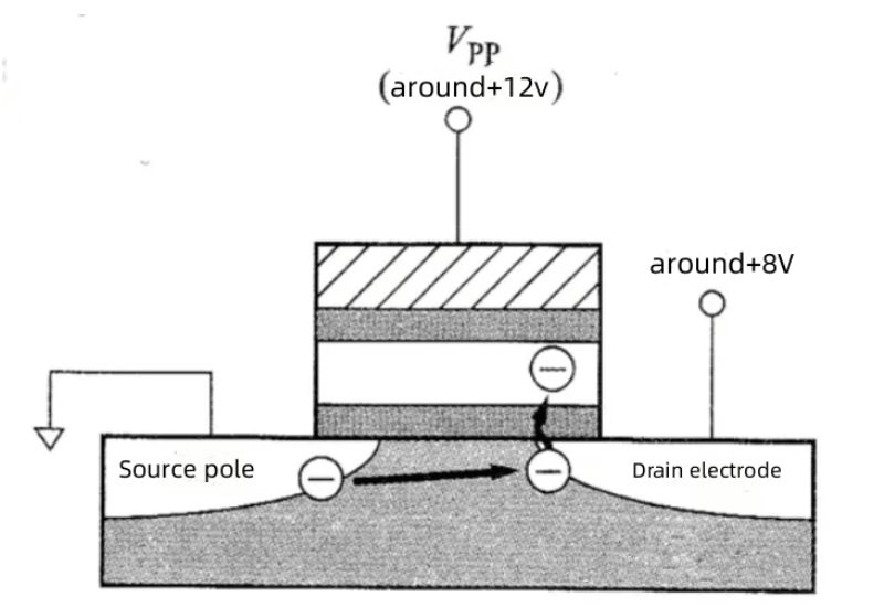
Today we will briefly talk about the principle of UV light erasure of wafer machines. When writing data, it is necessary to inject charge into the floating gate by applying a high voltage VPP to the gate, as shown in the figure below. Since the injected charge does not have the energy to penetrate the energy wall of the silicon oxide film, it can only maintain the status quo, so we must give the charge a certain amount of energy! This is when ultraviolet light is needed.

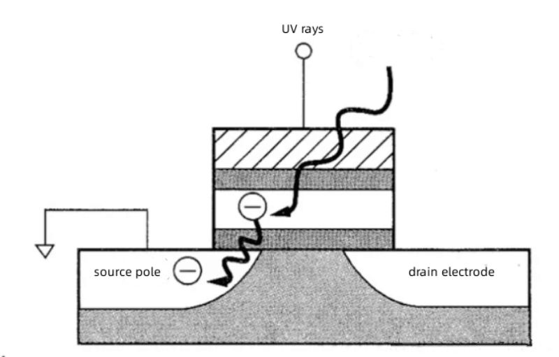
When the floating gate receives ultraviolet irradiation, the electrons in the floating gate receive the energy of ultraviolet light quanta, and the electrons become hot electrons with energy to penetrate the energy wall of the silicon oxide film. As shown in the figure, hot electrons penetrate the silicon oxide film, flow to the substrate and gate, and return to the erased state. The erasing operation can only be performed by receiving ultraviolet irradiation, and cannot be electronically erased. In other words, the number of bits can only be changed from "1" to "0", and in the opposite direction. There is no other way than erasing the entire contents of the chip.

We know that the energy of light is inversely proportional to the wavelength of light. In order for electrons to become hot electrons and thus have the energy to penetrate the oxide film, the irradiation of light with a shorter wavelength, that is, ultraviolet rays, is very much needed. Since the erasing time depends on the number of photons, the erasing time cannot be shortened even at shorter wavelengths. Generally, erasing starts when the wavelength is around 4000A (400nm). It basically reaches saturation around 3000A. Below 3000A, even if the wavelength is shorter, it will not have any impact on the erasing time.
The standard for UV erasure is generally to accept ultraviolet rays with a precise wavelength of 253.7nm and an intensity of ≥16000 μ W /cm². The erasure operation can be completed by exposure time ranging from 30 minutes to 3 hours.
Post time:2024-12-31 00:02:06

